![]()
222 Transverter
222 MHz Transverter Construction
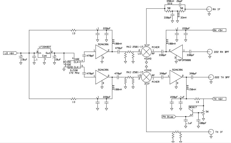
The IF frequency is 50 MHz. A 172 MHz LO is generated by a Silicon Labs Si530 chip. The differential outputs each drive a RFMD/Sirenza SGA-6386 chip to provide two buffered outputs. Each buffered LO output drives a double balanced diode mixer. A PDI MXJ-2501-17 (level 17, low conversion loss) is used in both the receive path and the up-conversion transmit path.
The receiver front-end consists of a Triquint 0.8 dB NF LNA, TQP3M9008, and two helical resonator BPF preselector. The preselector was constructed in a Hammond Aluminum housing. Insertion loss is 0.4 dB in the 15 MHz passband. Following the MXJ-2501 mixer is a matched band pass equalizer centered at 50 MHz.
The transmit circuit following the up conversion mixer is helical resonator BPF. This filter is identical to the receive preselector. A driver circuit consists of a RFMD/Sirenza SGA-6386. The power amplifier is a Mitsubishi RA30H2127M module. The 50 MHz IF signal is attenuated by a 30 dB power pad followed by an additional pi pad of surface mount resistors.
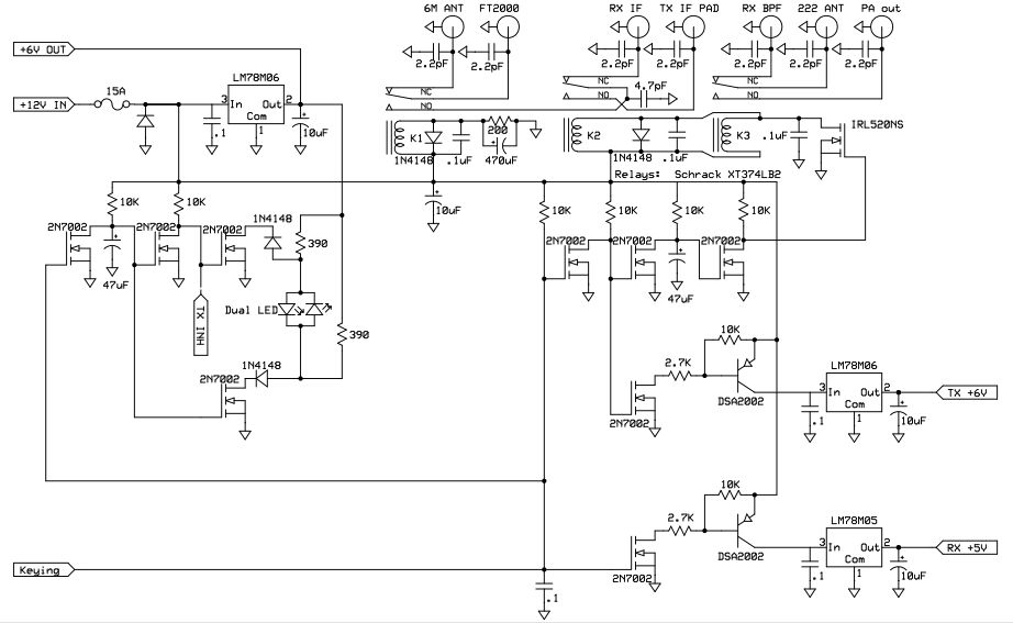
RF switching is provided by three, 12V, SPDT board mount relays. These are RP710012 made by Schrack. The path inductance is approximately 13 nH. All switched RF paths are compensated with shunt caps to form a pi LPF. Driver circuits for relay switching, sequencing, and switched bias circuits are all accomplished with self contained analog circuitry. When the transverter is in the OFF position the IF radio is switched to a 6M antenna port on the rear panel. A single +12V power supply is required for operation.
The front panel has a relative power output display. An RF voltage detector is integrated onto the PA module interface board at the rear panel. The detected voltage is displayed on an LED bar graph board from W6PQL. Jim has board kits available on his web site.
Due to limited number of 9913 coax runs to the antenna farm, 222 MHz and 50 MHz operation share a common feed. Home brew crossband couplers (band split diplexers) provide separate radio and antenna interfaces with only a few tenths of a dB loss and 60 dB of isolation. Operation at 200W on 6M is no problem due to use of transmitting micas.
![]()
222 Transverter - Top
![]()
222 Transverter - Rear
![]()
222 Transverter - Side
![]()
222 Transverter - Front Corner
222 Transverter - RF Board Schematic
222 Transverter - Bias & Control Schematic
![]()
222 Transverter - with Diplexer
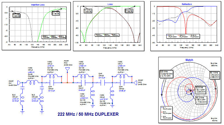
222 MHz Diplexer Design
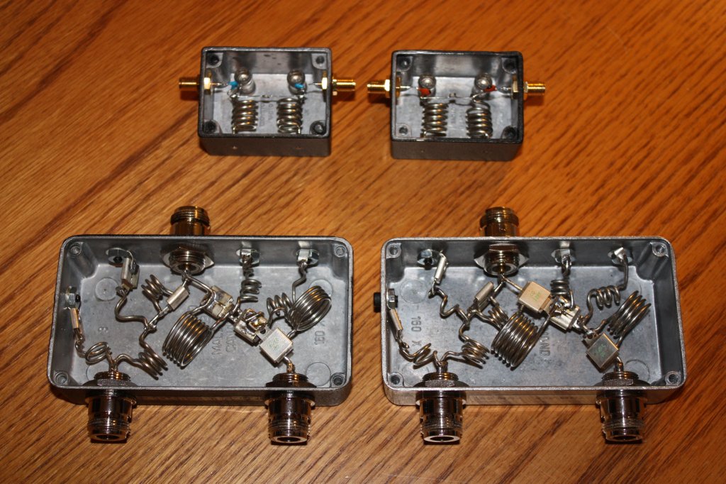
222 MHz BPF and 50 MHz - 222 MHz Diplexer Modules
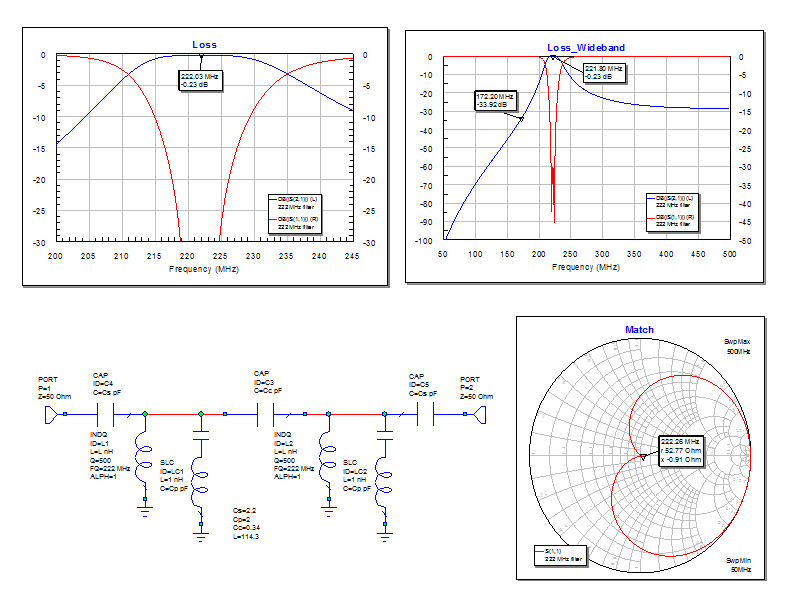
222 MHz Filter Design
222 Beacon
222 MHz Beacon Construction
The beacon RF chain begins with a Silicon Labs Si530 source at 222.060 MHz. The CW output operates at three power levels: full power, -10 dB, and -20 dB. The power stepping is accomplished by switching in pi pads with Analog Devices CMOS RF switches. The two differential outputs of the Si530 are used to obtain the first two level steps. An ADG-918 SPDT switch selects either a direct output or a 10 dB attenuated output. The ADG-918 provides termination of unselected port, so LO pulling when ports are switched is minimized. The lowest level is obtained by using an ADG919 and ADG918 to select a direct path or a 20 dB attenuated path. CW keying is accomplished by a combination of RF switching and DC switching of driver and PA bias. The RF switching is through a cascade of ADG-901 and ADG-902. The ADG-901 provides LO drive termination at all times. The driver is a RFMD/Sirenza SGA-6386 and the PA is a Mitsubishi RA30H2127M module. This PA is capable of 40 Watts; however, for reliable beacon duty it is run at 10W output. The control for CW keying and level steping is provided by a Freakin' Beacon FB-1 board.
![]()
222 Beacon - Interior
![]()
222 Beacon - RF Board Schematic
![]()
222 Beacon - Circuit Boards